


Analog Devices / Maxim Integrated MAX22515 IO-Link Transceiver
Analog Devices Inc. MAX22515 IO-Link Transceiver can operate as an IO-Link device in industrial applications. The MAX22515 features a selectable control interface (pin mode or I2C), two integrated linear regulators, and integrated surge protection for robust communication. The transceiver includes one C/Q input-output channel and one digital input (DI) channel. The device features a flexible control interface. Pin-control logic inputs allow for operation with switching sensors that do not use a microcontroller. For sensors that use a microcontroller, an I2C interface is available, providing extensive configuration and diagnostics. Additionally, an integrated oscillator simplifies the clock generation for IO-Link devices.
The MAX22515 features extensive integrated protection to ensure robust communication in harsh industrial environments. All IO-Link line interface pins (V24, C/Q, DI, and GND) are reverse voltage protected, short-circuit protected, hot-plug protected, and feature integrated ±1.2kV/500Ω surge protection. The Analog Devices Inc. MAX22515 IO-Link Transceiver is available in a tiny WLP package (2.5mm x 2.0mm) or a 24-pin TQFN-EP package (4mm x 4mm) and operates over the -40ºC to +125ºC temperature range.
Features
- High configurability and integration reduces SKU
- Operates from 8.0V to 36.0V
- Auxiliary digital input (DI)
- I2C or Pin mode vontrol
- 50mA to 250mA selectable C/Q driver current
- Selectable C/Q driver slew rate (I2C Mode)
- Integrated oscillator for IO-link Communication
- IO-Link Wake-Up Detection and wake-up generation
- 3.3V and 5.0V integrated linear regulators
- Compatible register set to MAX22513
- Integrated protection enables robust systems
- ±1.2kV/500Ω surge protection on V24, C/Q, DI, and GND
- Reverse oolarity protection on V24, C/Q, DI, and GND
- Hot-plug protection on supply input (V24)
- Glitch filters for improved burst resilience
- Selectable driver overcurrent configuration
- -40°C to +125°C operating temperature range
- Fast demagnetization of inductive loads
- Optimized for small designs
- 2Ω (typ) C/Q Driver On-Resistance power dissipation
- 1.3mA (typ) supply current
- Available in two tiny packages
- 20-bump WLP (2.5mm x 2.0mm)
- 24-pin TQFN-EP (4mm x 4mm)
Applications
- IO-link sensor and actuator devices
- Industrial sensors
- IO-link masters
Additional Resource
Simplified Block Diagram

Associated Development Tools
Analog Devices / Maxim Integrated MAXREFDES177 IO-Link Universal Analog IO
A complete, IO-Link® universal analog IO reference design with a MAX22515 IO-Link transceiver.

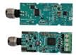
Analog Devices / Maxim Integrated MAX22515EVKIT Transceiver Evaluation Kit
Fully assembled & tested circuit board evaluates the MAX22515 IO-Link® dual-channel transceiver.